
Dr. Julien Pierce
Assistant Professor of Electrical & Computer Engineering
Instructor for EE 310, Fall 2026
- Office
- Rowan Engineering Center 218
- jpierce
@university.alkimi.ai
EE 310 · Electrical Engineering
Diodes, bipolar and field-effect transistors, amplifier biasing and small-signal models, frequency response, and feedback, with a weekly three-hour design laboratory.
Fall 2026 · At a glance
300-level courses: advanced, upper-division courses requiring prior foundational preparation. Counts toward the 36 upper-division credits every bachelor's degree requires (Undergraduate Catalog §2.3). Details: Undergraduate Catalog §9.21.
Assistant Professor of Electrical & Computer Engineering
Instructor for EE 310, Fall 2026
Questions about a major or your plan: Academic Advising Center, Lovell Hall 101, (555) 555-0158.
Class meetings
Lecture
Mon, Wed, Fri, 9:00–9:50 a.m.
Rowan Engineering Center 110
Lab
Mon, 1:00–3:50 p.m.
Rowan Engineering Center 150
Final exam
Wednesday, December 16, 2026
9:00–11:00 a.m., Rowan Engineering Center 110
Office hours
Mon & Fri, 11:30 a.m.–1:00 p.m.
Rowan Engineering Center 218
Wed, 3:00–4:00 p.m.
Virtual (Zoom link in Canvas)
Students may use AI assistants to generate LTspice circuit netlists, write Python or MATLAB scripts for plotting amplifier Bode frequency responses, and clarify solid-state semiconductor physics principles. AI models must not be used to perform analytical small-signal circuit calculations, calculate DC bias network resistor values on graded homework, or draft laboratory reports.
From the syllabus
Grading
Letter grades follow the university scale (Student Handbook §4.1).
Key dates
First day of classes Past
Midterm Exam 1 (Diodes & BJT Amplifiers) Next
Midterm Exam 2 (MOSFETs, Differential Pairs & Frequency)
Discrete Analog Audio Amplifier Design Project
Required materials
Sedra, Adel S., Kenneth C. Smith, Tony Chan Carusone, and Vincent Gaudet. Microelectronic Circuits. 8th ed., Oxford University Press, 2020.
Approx. $85 digital rental ($195 purchase; reserve copies available in Alkimi Library).
Analog parts kit and breadboard package (available in campus bookstore or department distribution).
Approx. $35.
Degree planning
What to take first, what this course opens up, and the requirements it can satisfy, from the Undergraduate Catalog.
Catalog wording: EE 201.
Every course also counts toward the 120 credits needed for a bachelor's degree. Confirm your plan with your advisor or the Academic Advising Center.
No AP exam awards credit for EE 310 (Undergraduate Catalog §3.11).
Registration
EE 310 is offered in the fall semester. Register through AlkimiHub self-service registration, which opens by credit standing. Until the add deadline, you don't need instructor permission as long as seats remain and you've met the prerequisites. Details: Student Handbook §3.3.
When a seat opens, AlkimiHub offers it to the first student on the waitlist and emails you. You have 24 hours to claim it before it goes to the next student. Details: Student Handbook §3.10.
Fall 2026 withdrawal deadline
Last day to withdraw with a W or elect Pass/No Pass.
Fall 2027 registration opens
By credit standing, in AlkimiHub.
The Fall 2026 add deadline passed on Sep 2, 2026.
All dates: academic calendar. Registration help: Office of the Registrar.
Official course syllabus
The syllabus as filed with the department and posted in Canvas for Fall 2026.
Term: Fall 2026
Credits: 4.0
Lecture Times & Location: Monday, Wednesday, Friday 9:00–9:50 a.m., Rowan Engineering Center 110
Laboratory Time & Location: Monday 1:00–3:50 p.m., Rowan Engineering Center 150
Modality: In-Person Lecture and Laboratory
jpierce@university.alkimi.ai
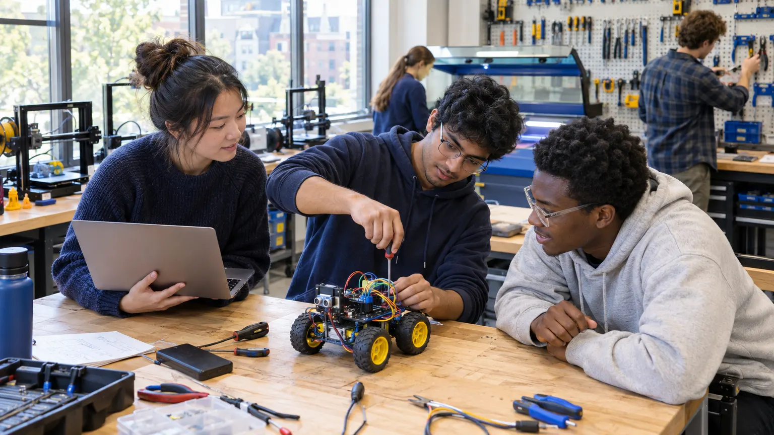
Diodes, bipolar and field-effect transistors, amplifier biasing and small-signal models, frequency response, and feedback, with a weekly three-hour design laboratory. EE 310 presents the fundamental principles of analog electronic circuit design, bridging semiconductor device physics with practical linear amplifier architectures. Students examine the operation, large-signal models, and small-signal linearizations of junction diodes, bipolar junction transistors (BJTs), and metal-oxide-semiconductor field-effect transistors (MOSFETs). The course emphasizes single- and multi-stage amplifier design, differential pairs, high-frequency response, feedback theory, and hands-on laboratory prototyping using discrete transistors and test instrumentation.
EE 201.
Upon successful completion of EE 310, students will be able to:
In accordance with Alkimi University Academic Policies (Student Handbook §5.8), EE 310 operates under AI Level 2.
| Week | Dates | Topics & Readings | Laboratory | Assignments & Deadlines |
|---|---|---|---|---|
| Week 1 | Aug 26, 28 | Amplifiers and Semiconductor Fundamentals: Course introduction, amplifier signal models, frequency response concepts, intrinsic semiconductors, doping, drift and diffusion currents, and the PN junction. Reading: Sedra & Smith Ch. 1, 3.1–3.3 | No lab meetings this week. | First day of classes: Wed Aug 26. |
| Week 2 | Aug 31–Sep 4 | Diode Characteristics and Modeling: Terminal I-V characteristics, temperature dependence, piecewise-linear and constant-voltage-drop models, and small-signal diode incremental resistance. Reading: Sedra & Smith Ch. 3.4–3.6 | Lab 1: PN Junction Diode I-V Curves and Rectifier Circuits | Wed Sep 2: Add/section change deadline. |
| Week 3 | Sep 9, 11 | Diode Circuits and Power Regulation: Half-wave and full-wave bridge rectifiers, capacitive filtering, ripple voltage calculations, Zener diode breakdown, and linear voltage regulation. Reading: Sedra & Smith Ch. 3.7–3.9 | No lab meetings this week (holiday). | Mon Sep 7: Labor Day (no classes). Wed Sep 9: Census date (last day to drop without a W). |
| Week 4 | Sep 14–18 | Bipolar Junction Transistors: Device Physics: Physical operation of NPN and PNP transistors, active mode currents, Early effect, collector curves, and saturation and cutoff operating boundaries. Reading: Sedra & Smith Ch. 6.1–6.2 | Lab 2: Zener Diode Regulation and Diode Wave-Shaping Circuits | — |
| Week 5 | Sep 21–25 | BJT DC Biasing and Small-Signal Models: Four-resistor bias networks, bias stability against beta variation, hybrid-pi and T small-signal models, and transconductance calculations. Reading: Sedra & Smith Ch. 6.3–6.4 | Lab 3: BJT Characteristic Curves and Bias Network Stability | — |
| Week 6 | Sep 28–Oct 2 | BJT Amplifier Configurations and Midterm Exam 1: Common-emitter, common-base, and common-collector (emitter-follower) amplifiers, gain and impedance derivations, and Midterm Exam 1 in Friday lecture. Reading: Sedra & Smith Ch. 6.5–6.6 | Lab 4: Single-Stage Common-Emitter BJT Amplifier Design | Midterm Exam 1 (Diodes & BJT Amplifiers) (in class). |
| Week 7 | Oct 5–9 | MOSFET Device Physics and Characteristics: MOS capacitor, enhancement NMOS and PMOS operation, drain current equations in triode and saturation regions, channel-length modulation, and body effect. Reading: Sedra & Smith Ch. 5.1–5.2 | Lab 5: MOSFET I-V Characterization and Current-Voltage Scaling | — |
| Week 8 | Oct 14, 16 | MOSFET DC Biasing and Small-Signal Operation: MOSFET biasing circuits, current mirror biasing, small-signal models, and transconductance calculation in saturation. Reading: Sedra & Smith Ch. 5.3–5.5 | No lab meetings this week (holiday). | Oct 12–Oct 13: Fall break (no classes). |
| Week 9 | Oct 19–23 | MOSFET Amplifier Topologies: Common-source amplifiers with resistive and active loads, source-followers (common-drain), common-gate stages, and swing limits. Reading: Sedra & Smith Ch. 5.6–5.7 | Lab 6: Common-Source MOSFET Amplifier with Active Load | — |
| Week 10 | Oct 26–30 | Differential Amplifiers and Active Loads: BJT and MOS differential pairs, common-mode and differential-mode gains, CMRR, Wilson current sources, and active loads. Reading: Sedra & Smith Ch. 8.1–8.4 | Lab 7: BJT Differential Pair and Current Mirror Active Loads | — |
| Week 11 | Nov 2–6 | Amplifier Frequency Response and Midterm Exam 2: Low-frequency response due to coupling/bypass capacitors, high-frequency transistor capacitance, Miller effect, and Midterm Exam 2 in Friday lecture. Reading: Sedra & Smith Ch. 9.1–9.5 | Lab 8: Frequency Response and High-Frequency Roll-Off Measurement | Fri Nov 6: Last day to withdraw (W) or elect Pass/No Pass. Midterm Exam 2 (MOSFETs, Differential Pairs & Frequency) (in class). |
| Week 12 | Nov 9–13 | Feedback Amplifier Principles and Stability: General feedback structure, advantages of negative feedback, the four basic feedback topologies, closed-loop gain stability, and Nyquist stability criterion. Reading: Sedra & Smith Ch. 11.1–11.5 | Lab 9: Closed-Loop Negative Feedback and Gain-Bandwidth Trade-Off | — |
| Week 13 | Nov 16–20 | Operational Amplifier Internal Circuitry: Internal stages of the classic 741 op-amp, input differential stage, intermediate gain stage, class-AB output stage, and slew-rate limits; Project due Friday. Reading: Sedra & Smith Ch. 12.1–12.4 | Lab 10: Op-Amp Non-Idealities: Offset Voltage, Bias Current, and Slew Rate | Discrete Analog Audio Amplifier Design Project due Fri Nov 20 at 11:59 p.m. |
| Week 14 | Nov 23 | Power Amplifiers and Output Stages: Classification of output stages: Class A, Class B push-pull, Class AB bias networks, crossover distortion, power conversion efficiency, and thermal heat sinks. Reading: Sedra & Smith Ch. 13.1–13.4 | Lab 11: Class AB Complementary Push-Pull Power Output Stage | Nov 25–Nov 27: Thanksgiving break (no classes). |
| Week 15 | Nov 30–Dec 4 | Sinusoidal Oscillators and Waveform Generators: Barkhausen stability criterion for oscillation, RC phase-shift oscillators, Wien-bridge circuits, LC tuned oscillators, and 555 astable multivibrators. Reading: Sedra & Smith Ch. 15.1–15.4 | Lab 12: Wien-Bridge Sine Wave Oscillator and Waveform Generation | — |
| Week 16 | Dec 7, 9 | Course Synthesis and Final Examination Review: Review of analog design trade-offs, device biasing, multistage frequency responses, feedback topologies, and final exam preparation. Reading: Review Sedra & Smith Ch. 3, 5, 6, 8, 9, 11 | Lab 13: Analog Audio Amplifier Project Demonstration and Characterization | Wed Dec 9: Last day of classes. Thu Dec 10: Reading Day. |
| Finals | Dec 16 | Comprehensive Final Examination: Wednesday, December 16, 2026, 9:00–11:00 a.m., Rowan Engineering Center 110. | — | Comprehensive. |
Punctual attendance at all lectures and laboratory sessions is mandatory. Hands-on bench experiments in Rowan Engineering Center 150 require safety compliance, circuit debugging skills, and collaborative teamwork that cannot be made up independently. If illness or approved university business necessitates an absence, contact Dr. Pierce before the session. Students who miss the first two class meetings without notifying the instructor may be dropped. Students may miss class for religious observance without penalty if they notify the instructor in writing within the first two weeks of the semester (by Wednesday, September 9, 2026). Absences for university-sponsored activities (athletics, performances, conferences) are excused with a letter from the sponsoring office at least one week in advance.
Weekly problem sets submitted after the deadline will be deducted 15% per day up to 48 hours late, after which solutions are released and no credit can be awarded. Laboratory reports submitted after Sunday 11:59 p.m. will incur a 10% penalty per 24 hours. The lowest homework and lowest lab report grades are dropped to account for emergencies.
The final examination (Wednesday, December 16, 2026, 9:00–11:00 a.m.) is scheduled by the University Registrar and can't be moved without the Dean's written approval (Faculty Handbook §5.5). A student with three or more final exams on the same calendar day may reschedule one of them. Requests go to the instructor of the middle exam by the last day of classes. For this term, send the request by Wednesday, December 9, 2026 (Student Handbook §6.4).
Alkimi University is an academic community devoted to rigorous scholarship, open intellectual inquiry, and uncompromising ethical conduct. All students are subject to the regulations of the Alkimi University Academic Integrity Policy. Academic dishonesty—including plagiarism, cheating on examinations, unauthorized collaboration, fabrication of empirical data, and unauthorized submission of academic work generated by artificial intelligence—undermines the integrity of the university and carries severe disciplinary sanctions. Sanctions range from a failing grade on an assignment or exam to an administrative course failure recorded as an 'XF' on the official transcript, academic suspension, or expulsion. Suspected violations are formally investigated and resolved through the Office of Academic Integrity in accordance with Faculty Handbook §6. For detailed information, consult the Office of Academic Integrity, Lovell Hall 315, (555) 555-0163, integrity@university.alkimi.ai.
Alkimi University is committed to providing equitable educational access and reasonable accommodations for all students with documented disabilities, including physical, sensory, psychological, learning, and chronic health conditions. Students requesting academic accommodations must formally register with the Office of Accessibility Services, Harlan Hall 204, (555) 555-0155, access@university.alkimi.ai. Once approved, students will receive an official Faculty Accommodation Letter detailing approved accommodations. Students should present this letter to the instructor as early in the semester as possible, and at least one week prior to any exam or assignment requiring accommodation. Accommodations cannot be applied retroactively.
Your physical health, psychological well-being, and mental health are essential to your academic success. If you experience heightened stress, anxiety, depressive symptoms, personal trauma, or academic burnout, free, confidential counseling and medical care are available through the Hollis Health & Counseling Center, located in the Hollis Center. Routine appointments are available Monday–Friday 8:00 a.m.–6:00 p.m. and Saturday 10:00 a.m.–2:00 p.m. during the semester by calling (555) 555-0190 or emailing health@university.alkimi.ai. Urgent, 24/7 crisis psychological counseling is accessible immediately at (555) 555-0199.
advising@university.alkimi.ai
askalibrarian@university.alkimi.ai
health@university.alkimi.ai
EE courses